On Friday (August 12), local time, the U.S. Department of Commerce’s Bureau of Industry and Security (BIS) disclosed in the Federal Register a new interim final rule on export restrictions that restricts the design of GAAFET (Full Gate Field Effect Transistor). ) EDA/ECAD software necessary for structural integrated circuits; ultra-wide bandgap semiconductor materials represented by diamond and gallium oxide; four technologies such as pressure gain combustion (PGC) used in gas turbine engines to implement new export controls, the effective date of the ban for today (August 15).
Among the four technologies, EDA is the most eye-catching, which is interpreted by the market as further restrictions on China’s chip industry by the United States after the “Chip and Science Act”, which directly affects domestic companies that design 3nm and more advanced chip products. However, 3-nanometer design is rarely used in China at present, and its short-term impact is limited.
In addition to the 3nm process, 800V fast charging may be affected
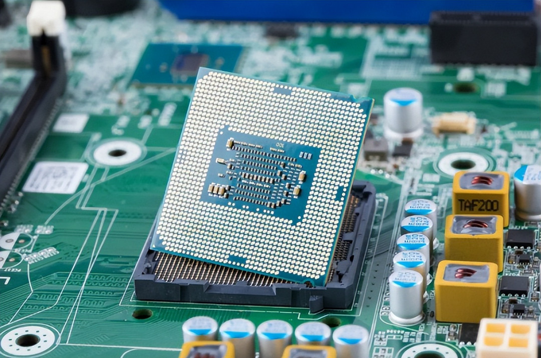
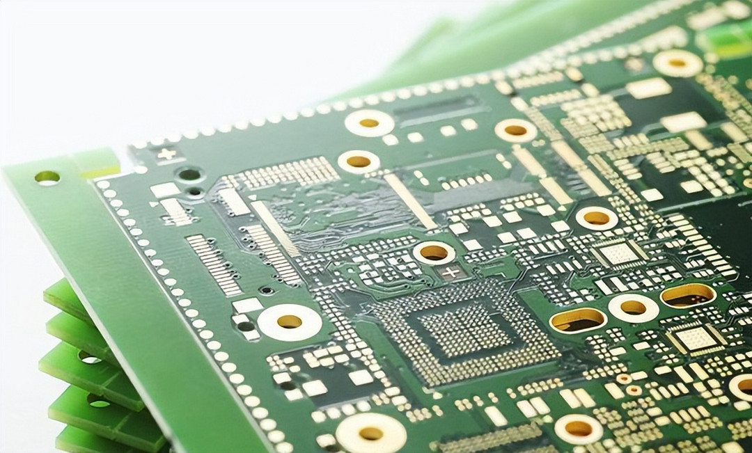
EDA (Electronics Design Automation) is electronic design automation, which is an indispensable and important part of chip IC (integrated circuit) design. It belongs to the upstream industry of chip manufacturing, covering all processes such as integrated circuit design, wiring, verification and simulation. EDA is called the “mother of chips” in the industry.
Tianfeng International Research Report pointed out that if chip manufacturing is compared to building a building, IC design is a design drawing, and EDA software is a design tool for drawings, but EDA software is much more complex than architectural design software.
ECAD (Electronic Computer Aided Design software) has a wider scope than EDA, and the ban means that all related software is covered. According to the U.S. Department of Commerce, ECAD is a class of software tools used to design, analyze, optimize and verify the performance of an integrated circuit or printed circuit board. Used to design complex integrated circuits in a variety of applications in the military, aerospace, and defense industries.
GAAFET transistor technology is a more advanced technology compared to FinFET transistors (fin field effect transistors), FinFET technology can achieve up to 3 nanometers, while GAAFET can achieve 2 nanometers.
This is the third export control initiated by the United States against China in the field of EDA. The first was against ZTE in 2018 and the second was against Huawei in 2019. In addition to consumer electronics such as Apple mobile phones and computers, the chips using the most advanced manufacturing process on the market are all chips with high computing power, such as GPUs used for artificial intelligence, and server chips used in data centers and cloud computing.
Some chip designers said that the short-term impact of this control measure is limited, because 3-nanometer designs are rarely used in China. Some AI chips and GPU chips use 7-nanometers, while TVs, set-top boxes, and automotive-grade chips are mostly 28 nm. nanometer or 16 nanometer. Some industry observers believe that the United States wants to make the Chinese mainland have no tools to design high-end chips of 3 nanometers and below, and the design is stuck at 5 nanometers, and the manufacturing is stuck at 7 nanometers. Then, the distance between China and the United States in high-speed computing, artificial AI, etc. will be widened.
In the opinion of a chip person, the core reason why the United States suppresses EDA is to control the production capacity of domestic chips.
In addition to the EDA software this time, two semiconductor materials are also involved: gallium oxide (Ga2O3) and diamond substrates, both of which are ultra-wide bandgap semiconductor materials. Such materials are expected to work under harsher conditions, such as higher voltages or higher temperatures.
These materials are still in development and have not been industrialized on a large scale, and the technology is mainly concentrated in Japan and the United States. However, chips made of these materials will be more suitable for multiple industrial environments such as new energy, grid energy storage, communications, etc., and therefore become very sensitive and important.
Taking new energy vehicles as an example, at present, new energy vehicle companies such as Xiaopeng Motors, BYD, Li Auto, and BAIC Jihu have already deployed 800V fast charging technology, and will be mass-produced around this year. Power devices made of gallium oxide materials can be used in these fast charging technologies.
Domestic EDA “breakthrough” opportunity
“If you design a 5-nanometer chip product and use the world’s top EDA software, the cost can be controlled at about 40 million US dollars, but without EDA software support, the cost of designing a 5-nanometer chip may be as high as 7.7 billion US dollars. The US dollar is close to a gap of about 200 times.” The relevant person in charge of a domestic CAD (computer-aided design) software company calculated an account.

At present, the global market concentration of the EDA industry is relatively high. The three EDA giants Synopsys (Synopsys), Cadence (Kedence Electronics), and Mentor Graphics (Mentor International, acquired by Siemens in Germany in 2016) firmly occupy more than 70% of the global market. market share, and can provide complete EDA tools, covering the whole process or most of the process of integrated circuit design and manufacturing.
The three companies have their own characteristics in products, and the focus and advantages of IP (intellectual property) are quite different. Their products have a market share of 85% in China. The 3-nanometer GAAFET architecture process technology that Samsung just broke through in June this year was completed with the assistance of Synopsys and Cadence.
The second-tier companies are represented by ANSYS, Silvaco, Aldec Inc, Huada Jiutian, etc. They have the entire process in specific fields and are more advanced in technology in local fields. Companies in the third echelon include Altium, Concept Engineering, Introduction Electronics, Guangliwei, Sierxin, DownStream Technologies, etc. The layout of EDA is mainly based on point tools, and there is a lack of full-process products in specific fields.
Most domestic chip design companies still use imported EDA industrial software to design chips. In 1993, Huada Jiutian released the first domestic EDA software – Panda ICCAD system, which achieved a breakthrough in domestic EDA from 0 to 1. In 2020, in China’s EDA market, in terms of revenue scale, Huada Jiutian ranked fourth.
On July 29, Huada Jiutian officially landed on the Growth Enterprise Market, with an increase of 126% on the first day of listing, and its market value exceeded 40 billion yuan. Huada Jiutian stated in the prospectus that most of its digital circuit design EDA products can support the 5-nanometer process; Gelun Electronics stated in its annual report that some tools can support the 7-nanometer, 5-nanometer, and 3-nanometer processes.
Huada Jiutian’s revenue in 2021 is 580 million yuan, and the revenue of Gailun Electronics is less than 200 million yuan. The world’s No. 1 Synopsys has a revenue of about 26 billion yuan and a profit of more than 5 billion yuan.
Tianfeng International Research Report pointed out that localization is imperative. There are about 40 sub-sectors in the EDA tool chain. The three giants have achieved the coverage of the entire industry chain, while the domestic leader Huada Jiutian currently has a coverage rate of about 40%. Others The products of domestic EDA manufacturers are mostly point tools.
According to statistics, there are about 100 design tool companies in China. EDA is divided into analog chip design tools and digital chip design tools. Some domestic companies have solved the whole process of designing analog chips. Design tools for digital chips are more difficult. About 120 “point tools” are involved in the design process, and research and development are carried out on each point tool.
There is a view that for the containment of the United States, the only way to improve the level of domestic EDA software is to quickly improve the level of domestic EDA software, and domestic enterprises should unite, and even Huawei HiSilicon and domestic universities should participate in forming alliances for joint development. With the increasing demand for domestic chips, domestic EDA is not without opportunities in the buyer’s market.
Post time: Aug-15-2022